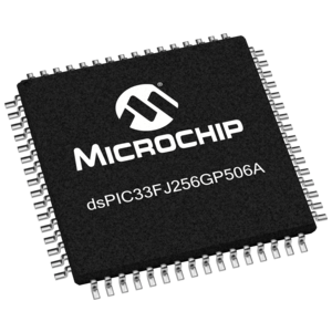
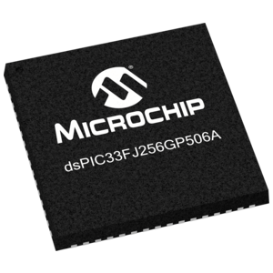
DSPIC33FJ256GP506A
40 MIPS, 256KB Flash, 16KB RAM, 64 pins, CAN
制造商:
产品信息
dsPIC33FJXXXGPXXXA General Purpose Digital Signal Controller (DSC) with seamless migration options to PIC24 MCUs and dsPIC30F DSCs in similar packages. These devices are available in extended operating temperature options
Operating Range:DC – 40 MIPS (40 MIPS @ 3.0-3.6V, -40°C to +85°C)
DC – 40 MIPS (40 MIPS @ 3.0-3.6V, -40°C to +125°C)
Industrial temperature range (-40°C to +85°C)
Extended temperature range (-40°C to +125°C)
High temperature range (-40°C to +140°C)High-Performance DSC CPU:
Modified Harvard architecture
C compiler optimized instruction set
16-bit wide data path
24-bit wide instructions
Linear program memory addressing up to 4M instruction words
Linear data memory addressing up to 64 Kbytes
83 base instructions: mostly 1 word/1 cycle
Sixteen 16-bit General Purpose Registers
Two 40-bit accumulators:- With rounding and saturation options
Flexible and powerful addressing modes:- Indirect, Modulo and Bit-Reversed
Software stack
16 x 16 fractional/integer multiply operations
32/16 and 16/16 divide operations
Single-cycle multiply and accumulate:- Accumulator write back for DSP operations- Dual data fetch
Up to ±16-bit shifts for up to 40-bit dataDirect Memory Access (DMA):
8-channel hardware DMA:
2 Kbytes dual ported DMA buffer area (DMA RAM) to store data transferred via DMA:- Allows data transfer between RAM and a peripheral while CPU is executing code (no cycle stealing)
Most peripherals support DMAInterrupt Controller:
5-cycle latency
118 interrupt vectors
Up to 67 available interrupt sources
Up to 5 external interrupts
7 programmable priority levels
5 processor exceptionsDigital I/O:
Wake-up/Interrupt-on-Change on up to 24 pins
Output pins can drive from 3.0V to 3.6V
All digital input pins are 5V tolerant
4 mA sink on all I/O pinsSystem Management:
Flexible clock options:- External, crystal, resonator, internal RC- Fully integrated PLL- Extremely low jitter PLL
Power-up Timer
Oscillator Start-up Timer/Stabilizer
Watchdog Timer with its own RC oscillator
Fail-Safe Clock Monitor
Reset by multiple sourcesPower Management:
On-chip 2.5V voltage regulator
Switch between clock sources in real time
Idle, Sleep and Doze modes with fast wake-upTimers/Capture/Compare/PWM:
Timer/Counters, up to nine 16-bit timers:- Can pair up to make four 32-bit timers- 1 timer runs as Real-Time Clock with external 32.768 kHz oscillator- Programmable prescaler
Input Capture (up to 8 channels):- Capture on up, down or both edges- 16-bit capture input functions- 4-deep FIFO on each capture
Output Compare (up to 8 channels):- Single or Dual 16-Bit Compare mode- 16-bit Glitchless PWM modeCommunication Modules:
3-wire SPI (up to 2 modules):- Framing supports I/O interface to simple codecs- Supports 8-bit and 16-bit data- Supports all serial clock formats and sampling modes
I2C™ (up to 2 modules):- Full Multi-Master Slave mode support- 7-bit and 10-bit addressing- Bus collision detection and arbitration- Integrated signal conditioning- Slave address masking
UART (up to 2 modules):- Interrupt on address bit detect- Interrupt on UART error- Wake-up on Start bit from Sleep mode- 4-character TX and RX FIFO buffers- LIN bus support- IrDA® encoding and decoding in hardware- High-Speed Baud mode- Hardware Flow Control with CTS and RTS
Data Converter Interface (DCI) module:- Codec interface- Supports I2S and AC’97 protocols- Up to 16-bit data words, up to 16 words per frame- 4-word deep TX and RX buffers
Enhanced CAN (ECAN™ module) 2.0B active (up to 2 modules):- Up to 8 transmit and up to 32 receive buffers- 16 receive filters and 3 masks- Loopback, Listen Only and Listen All Messages modes for diagnostics and bus monitoring- Wake-up on CAN message- Automatic processing of Remote Transmission Requests- FIFO mode using DMA- DeviceNet™ addressing supportAnalog-to-Digital Converters (ADCs):
Up to two ADC modules in a device
10-bit, 1.1 Msps or 12-bit, 500 Ksps conversion:- 2, 4 or 8 simultaneous samples- Up to 32 input channels with auto-scanning- Conversion start can be manual or synchronized with 1 of 4 trigger sources- Conversion possible in Sleep mode- ±2 LSb max integral nonlinearity- ±1 LSb max differential nonlinearityCMOS Flash Technology:
Low-power, high-speed Flash technology
Fully static design
3.3V (±10%) operating voltage
Industrial temperature
Extended temperature
Low-power consumption
在线购买
型号:DSPIC33FJ256GP506AT-E/PT
描述:-
型号:DSPIC33FJ256GP506AT-E/MR
描述:-
型号:DSPIC33FJ256GP506A-E/MR
描述:-
型号:DSPIC33FJ256GP506AT-I/PT
描述:-
型号:DSPIC33FJ256GP506AT-I/MR
描述:-
型号:DSPIC33FJ256GP506A-I/MR
描述:-
应用案例
高性能电机控制单片机— dsPIC33EP256MC506 系列
2018-06-08
脉搏血氧仪演示板
2018-06-06
MPLAB代码配置器实验5
2018-06-06
Microchip PIC24FJ256DA210开发板在图形显示上的应用
2018-06-06
基于Microchip dsPIC33CK256MP506 高性能DSP开发的3.3KW双向图腾柱PFC逆变电源方案
2025-01-17
扬杰科技SOT-227 FJ封装车载模块介绍
2022-05-27
基于Microchip产品的4KW图腾柱PFC数字电源方案
2022-04-22
高级16位数字信号控制器dsPIC33F的主要特性及应用电路
2021-03-30


