STLC2690
3蓝牙和FM RDS收发器芯片系统
制造商:
产品信息
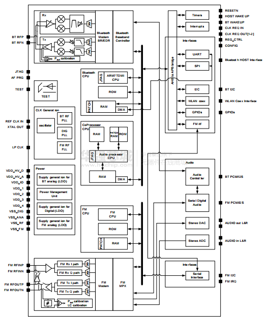
The STLC2690 combines Bluetooth and FM transceiver functionality on a single chip and is fully optimized for mobile applications such as mobile phones, smart phones, PDAs and portable media players. The required board space has been minimized, power consumption levels are targeted for battery powered devices and the integration allows a cost effective solution. Amongst others the reduction of external components enables manufacturers to easily and fast integrate the STLC2690 on their product to enable a short time to market. Compared to its successful predecessor, the STLC2593, the STLC2690 is a system on chip device, it adds an FM transmitter, an audio processor and A2DP encapsulation and further optimizes in terms of RF performance and cost.
stlc2690结合在一个单芯片蓝牙和FM收发功能,全面优化的移动应用如手机、智能手机、PDA和便携式媒体播放器。所需的电路板空间已被最小化,功率消耗水平是针对电池供电设备和集成允许一个成本有效的解决方案。其他外部元件的减少使制造商能够轻松,快速融入stlc2690对他们的产品,使短时间内市场。相比其前身的成功,stlc2593,的stlc2690是芯片装置系统,它增加了一个FM发射器,音频处理器和射频性能和成本方面的A2DP封装和进一步优化。
Key Features
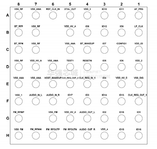
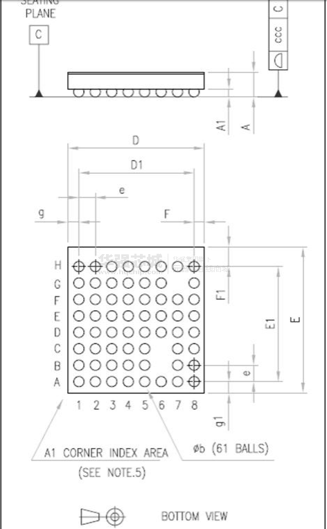
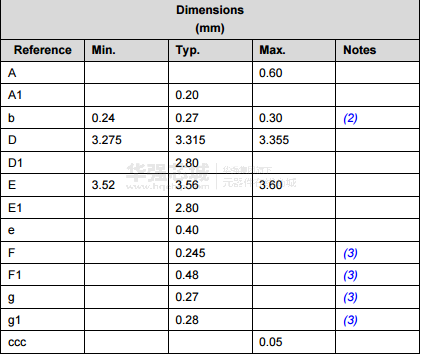
WLCSP 0.6 mm high, 0.4 mm pitch, lead-free/RoHs compliant, 61 pins
10 external components: 5 decoupling capacitors on the power supply, 1 B-BPF for Bluetooth, 1 inductor and 3 capacitors for FM RX
PCB footprint < 36 mm2
Clocks
Fast clock input (digital or sine wave) at 13, 16, 16.8, 19.2, 26, 32, 33.6, 38.4, 52 MHz
Slow clock input at 32, 32.768 kHz
Direct external crystal input
Power supply
Single power supply with internal regulators
1.65 V to 1.95 V I/O systems
Various on-chip auto calibration features (VCO, Filters, …)
主要特点
WLCSP 0.6毫米高,0.4毫米间距,无铅和符合RoHS标准,61针
10部分:5外部去耦电容在电源、蓝牙b-bpf 1,1和3电容电感调频接收
电路板面积<36平方毫米
时钟
快速时钟输入(数字或正弦波)在13,16,16.8,19.2,26,33.6,38.4,52,32兆赫
慢时钟输入在32,32.768千赫
直接外接晶体输入
电源供应
单一电源内部调节器
1.65伏到1.95伏的系统
各种芯片的自动校准功能(压控振荡器、滤波器、…)


