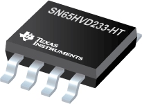
SN65HVD233-HT
高温 3.3V CAN 收发器
制造商:TI
产品信息
描述 The SN65HVD233 is used in applications employing the controller area network (CAN) serial communication physical layer in accordance with the ISO 11898 standard, with the exception that the thermal shutdown is removed. As a CAN transceiver, the device provides transmit and receive capability between the differential CAN bus and a CAN controller, with signaling rates up to 1 Mbps. Designed for operation in especially harsh environments, the device features cross wire, overvoltage, and loss-of-ground protection to ±36 V, with common-mode transient protection of ±100 V. This device operates over a 7-V to 12-V common-mode range with a maximum of 60 nodes on a bus. If the common-mode range is restricted to the ISO 11898 standard range of 2 V to 7 V, up to 120 nodes may be connected on a bus. This transceiver interfaces the single-ended CAN controller with the differential CAN bus found in industrial, building automation, and automotive applications. RS (pin 8) provides for three modes of operation: high-speed, slope control, or low-power standby mode. The high-speed mode of operation is selected by connecting RS directly to ground, thus allowing the driver output transistors to switch on and off as fast as possible with no limitation on the rise and fall slope. The rise and fall slope can be adjusted by connecting a resistor to ground at RS, because the slope is proportional to the output current of the pin. Slope control is implemented with a resistor value of 10 kΩ to achieve a slew rate of ≉ 15 V/µs, and a value of 100 kΩ to achieve ≉ 2 V/µs slew rate. For more information about slope control, refer to the Application and Implementation section. The SN65HVD233 enters a low-current standby mode, during which the driver is switched off and the receiver remains active if a high logic level is applied to RS. The local protocol controller reverses this low-current standby mode when it needs to transmit to the bus. A logic high on the loopback (LBK, pin 5) of the SN65HVD233 places the bus output and bus input in a high-impedance state. The remaining circuit remains active and available for the driver to receiver loopback, self-diagnostic node functions without disturbing the bus.特性Bus-Pin Fault Protection Exceeds ±36 VBus-Pin ESD Protection Exceeds 16-kV Human Body Model (HBM)Compatible With ISO 11898Signaling Rates(1) up to 1 MbpsExtended 7-V to 12-V Common-Mode RangeHigh-Input Impedance Allows for 120 NodesLVTTL I/Os Are 5-V TolerantAdjustable Driver Transition Times for Improved Signal QualityUnpowered Node Does Not Disturb the BusLow-Current Standby Mode: 200 µA TypicalPower-Up and Power-Down Glitch-Free Bus Inputs and Outputs High-Input Impedance With Low VCC Monolithic Output During Power CyclingLoopback for Diagnostic Functions AvailableDeviceNet™ Vendor ID #806(1)APPLICATIONSDown-Hole Drilling High-Temperature Environments Industrial AutomationDeviceNet Data Buses Smart Distributed Systems (SDS™) SAE J1939 Data Bus Interfaces NMEA 2000 Data Bus Interfaces ISO 11783 Data Bus Interfaces CAN Data Bus InterfacesControlled BaselineOne Assembly or Test SiteOne Fabrication SiteAvailable in Extreme (55°C to 210°C) Temperature Range2Extended Product Life CycleExtended Product-Change NotificationProduct TraceabilityTexas Instruments high-temperature products use highly optimized silicon (die) solutions with design and process enhancements to maximize performance over extended temperatures.(1) The signaling rate of a line is the number of voltage transitions that are made per second expressed in the units bps (bits per second). 2 Custom temperature ranges available All other trademarks are the property of their respective owners
在线购买
型号:SN65HVD233SKGDA
描述:-
型号:SN65HVD233SHKQ
描述:-
型号:SN65HVD233SJD
描述:-
型号:SN65HVD233HD
描述:-
型号:SN65HVD233SHKJ
描述:-

