MC74VHC1GT126
Single Non-Inverting Buffer, TTL Level
制造商:ON
产品信息
The MC74VHC1GT126 is a single gate noninverting 3-state buffer fabricated with silicon gate CMOS technology. It achieves high speed operation similar to equivalent Bipolar Schottky TTL while maintaining CMOS low power dissipation.
The MC74VHC1GT126 requires the 3-state control input (OE(bar)) to be set Low to place the output into the high impedance state. The device input is compatible with TTL-type input thresholds and the output has a full 5V CMOS level output swing. The input protection circuitry on this device allows overvoltage tolerance on the input, allowing the device to be used as a logic-level translator from 3.0V CMOS logic to 5.0V CMOS Logic or from 1.8V CMOS logic to 3.0V CMOS Logic while operating at the high-voltage power supply. The MC74VHC1GT126 input structure provides protection when voltages up to 7V are applied, regardless of the supply voltage. This allows the MC74VHC1GT126 to be used to interface 5V circuits to 3V circuits. The output structures also provide protection when V
= 0V. These input and output structures help prevent device destruction caused by supply voltage - input/output voltage mismatch, battery backup, hot insertion, etc.
- High Speed: t
- = 3.5ns (Typ) at V
- = 5V
- Low Power Dissipation: I
- = 1µA (Max) at T
- = 25°C
- TTL-Compatible Inputs: V
- = 0.8V; V
- = 2.0V
- CMOS-Compatible Outputs: V
- > 0.8V
- ; V
- CC @Load
- Power Down Protection Provided on Inputs and Outputs
- Balanced Propagation Delays
- Pin and Function Compatible with Other Standard Logic Families
- Chip Complexity: FETs = 62; Equivalent Gates = 16
- Pb-Free Packages are Available
电路图、引脚图和封装图
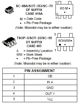
MC74VHC1GT126电路图
在线购买
型号:NLVVHC1GT126DF2G
描述:-
型号:NLVVHC1GT126DF1G
描述:-
型号:M74VHC1GT126DT1G
描述:-
型号:M74VHC1GT126DF2G
描述:-
型号:M74VHC1GT126DF1G
描述:-
型号:NLVVHC1GT126DT1G
描述:-
技术资料
应用案例
MC3303DG是什么芯片?
2023-09-05
74VHC123A双可重触发单稳态多谐振荡器:特性、应用与设计要点
2026-01-30
探索MC33171/72/74、NCV33172/
2025-11-27
用东芝74VHC74FT提升您的下一个项目:高速度、低功耗的CMOS双D触发器
2024-10-15
探索MC74HC595A与MC74HCT595A:8位移位寄存器的性能与应用解析
2025-11-27
双非反相施密特触发器缓冲器MC74VHC2G17和MC74VHC2GT17的特性与应用分析
2025-11-26
MC74VHC1G125/MC74VHC1GT125 3态缓冲器技术深度解析
2025-11-26
国芯思辰|用于投影仪的中微爱芯单路反相器AiP74LVC1G04可替代TI的SN74LVC1G04DCKR
2022-08-25