MC10E111
9 Differential Clock Driver
制造商:ON
产品信息
The MC10E/100E111 is a low skew 1-to-9 differential driver, designed with clock distribution in mind. It accepts one signal input, which can be either differential or else single-ended if theV
output is used. The signal is fanned out to 9 identical differential outputs. An enable input is also provided. A HIGH disables the device by forcing all Q outputs LOW and all Qbar outputs HIGH.
The device is specifically designed, modeled and produced with low skew as the key goal. Optimal design and layout serve to minimize gate to gate skew within-device, and empirical modeling is used to determine process control limits that ensure consistent tpd distributions from lot to lot. The net result is a dependable, guaranteed low skew device.
To ensure that the tight skew specification is met it is necessary that both sides of the differential output are terminated into 50 , even if only one side is being used. In most applications, all nine differential pairs will be used and therefore terminated. In the case where fewer than nine pairs are used, it is necessary to terminate at least the output pairs on the same package side (i.e. sharing the same V
) as the pair(s) being used on that side, in order to maintain minimum skew. Failure to do this will result in small degradations of propagation delay (on the order of 10-20 ps) of the output(s) being used which, while not being catastrophic to most designs, will mean a loss of skew margin.
The V
pin, an internally generated voltage supply, is available to this device only. For single-ended input conditions, the unused differential input is connected to V
as a switching reference voltage. V
may also rebias AC coupled inputs. When used, decoupleV
and V
via a 0.01 F capacitor and limit current sourcing or sinking to 0.5 mA. When not used, V
should be left open.
The 100 Series contains temperature
- Guaranteed Skew Spec
- Differential Design
- V
- Output
- PECL Mode Operating Range: V
- = 4.2 V to 5.7 V
- with V
- = 0 V
- NECL Mode Operating Range: V
- = 0 V
- with V
- = -4.2 V to -5.7 V
- Internal Input Pulldown Resistors
- ESD Protection: > 3 KV HBM
- Meets or Exceeds JEDEC Spec EIA/JESD78 IC Latchup Test
- Moisture Sensitivity Level 1 (For Additional Information, see Application Note AND8003/D)
- Flammability Rating: UL-94 code V-0 @ 1/8 inch, Oxygen Index 28 to 34
- Transistor Count = 178 devices
- Pb-Free Packages are Available
电路图、引脚图和封装图
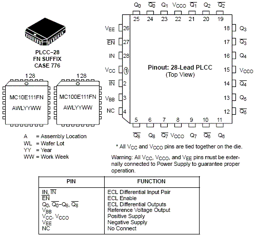
MC10E111电路图
应用案例
你也可以懂的质能方程E=mc²
2021-05-20
CDCLVP111-SP 低电压1:10 LVPECL可选择性输入时钟驱动器技术文档总结
2025-09-13
红旗E111换电过程曝光:全程不到1分钟
2021-02-01
比亚迪刀片电池上车!红旗全新纯电动轿车E111申报
2021-01-15
深入解析CDCLVP111-SEP:低电压1:10 LVPECL时钟驱动器
2026-02-06
探索MC111:25V单相位BLDC电机驱动芯片的卓越性能与应用
2026-01-06
坚固三防工业平板就选它:合亿 MC10 测评
2024-06-14
GP10/GP20/GM10重点功能--WT连接(WT1800R/WT500/WT300
2025-01-17