

MC100EP14
5 Differential, ECL / HSTL, 3.3 V / 5.0 V
制造商:ON
产品信息
The MC100EP14 is a low skew 1-to-5differential driver, designed with clock distribution in mind, accepting two clock sources into an inputmultiplexer. The ECL/PECL input signals can be either differential or single-ended (if the V
output is used). HSTL inputs can be used when the LVEP14 is operating under PECL conditions.
The EP14 specifically guarantees low output-to-output skew. Optimal design, layout, and processing minimize skew within a device and from device to device.
To ensure that the tight skew specification is realized, both sides of any differential output need to be terminated even if only one output is being used. If an output pair is unused, both outputs may be left open (unterminated) without affecting skew.
The common enable (ENbar) is synchronous, outputs are enabled/disabled in the LOW state. This avoids a runt clock pulse when the device is enabled/disabled as can happen with an asynchronous control. The internal flip flop is locked on the falling edge of the input clock, therefore all associated specification limits are referenced to the negative edge of the clock input.
The VBB pin, an internally generated voltage supply, is available to this device only. For single-ended input conditions, the unused differential input is connected to VBB as a switching reference voltage. VBB may also rebias AC coupled inputs. When used, decouple VBB and VCC via a 0.01 uF capacitor and limit current sourcing or sinking to 0.5 mA. When not used, VBB should be left open.
output is used). HSTL inputs can be used when the LVEP14 is operating under PECL conditions.
The EP14 specifically guarantees low output-to-output skew. Optimal design, layout, and processing minimize skew within a device and from device to device.
To ensure that the tight skew specification is realized, both sides of any differential output need to be terminated even if only one output is being used. If an output pair is unused, both outputs may be left open (unterminated) without affecting skew.
The common enable (ENbar) is synchronous, outputs are enabled/disabled in the LOW state. This avoids a runt clock pulse when the device is enabled/disabled as can happen with an asynchronous control. The internal flip flop is locked on the falling edge of the input clock, therefore all associated specification limits are referenced to the negative edge of the clock input.
The VBB pin, an internally generated voltage supply, is available to this device only. For single-ended input conditions, the unused differential input is connected to VBB as a switching reference voltage. VBB may also rebias AC coupled inputs. When used, decouple VBB and VCC via a 0.01 uF capacitor and limit current sourcing or sinking to 0.5 mA. When not used, VBB should be left open.
- 400 ps Typical Propagation Delay
- 100 ps Device-to-Device Skew
- 25 ps Within Device Skew
- Maximum Frequency > 2 GHz Typical
- The 100 Series Contains Temperature Compensation
- PECL and HSTL Mode: V
- = 3.0 V to 5.5 V with V
- = 0 V
- NECL Mode: V
- = 0 V with V
- = -3.0 V to -5.5 V
- Open Input Default State
电路图、引脚图和封装图
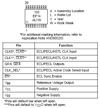
MC100EP14电路图
技术资料
应用案例
MC/DC:与100%覆盖率的斗争
2022-11-05
MC/DC:与100%覆盖率的斗争
2022-11-05
Onsemi MC10EP57和MC100EP57:高性能差分复用器的技术剖析
2026-08-28
Onsemi MC10EP05和MC100EP05:高性能2输入差分与/与非门解析
2026-08-27
MC/DC:与100%覆盖率的斗争
2022-11-05
Onsemi MC10EP105/MC100EP105:高性能ECL逻辑门的详细解析
2026-08-27
解析 onsemi MC100EP14:高性能时钟驱动芯片的应用指南
2026-08-26
深入剖析 onsemi MC10EP11/MC100EP11 差分扇出缓冲器
2026-08-26
