MC100EL91
Triple LVPECL/PECL Input to -5.0 V ECL Output Translator
制造商:ON
产品信息
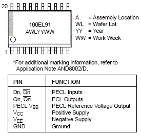
The MC100EL91 is a triple PECL input to ECL output translator. The device receives standard or low voltage differential PECL signals, determined by the V
supply level, and translates them to differential -5 V ECL output signals. (For translation to -3.3 V ECL output, see MC100LVEL91.)
To accomplish the level translation, the EL91 requires three power rails. The V
supply should be connected to the positive supply, and the V
pin should be connected to the negative power supply. The GND pins are connected to the system ground plane. Both V
and V
should be bypassed to ground via 0.01 µF capacitors. Under open input conditions, the Dbar input will be biased at V
/2 and the D input will be pulled to GND. This condition will force the Q output to a low, ensuring stability. The V
pin, an internally generated voltage supply, is available to this device only. For single-ended input conditions, the unused differential input is connected to V
as a switching reference voltage. V
may also rebias AC coupled inputs. When used, decouple V
and V
via a 0.01 µF capacitor and limit current sourcing or sinking to 0.5 mA. When not used, V
should be left open.
- 670 ps Typical Propagation Delay
- ESD Protection: >2 KV HBM, >200 V MM
- The 100 Series Contains Temperature Compensation
- Operating Range: V
- = 4.75 V to 5.25 V;
- V
- = -4.2 V to -5.5 V; GND= 0 V
- Internal Input Pulldown Resistors
- Q Output will Default LOW with Inputs Open or at V
- Flammability Rating: UL-94 code V-0 @ 1/8",
- Oxygen Index 28 to 34
- Transistor Count = 282 devices
- Pb-Free Packages are Available

