MC100EL15
4 ECL, 5.0 V
制造商:ON
产品信息
The MC10EL/100EL15 is a low skew 1:4 clock distribution chip designed explicitly for low skew clock distribution applications. The device can be driven by either a differential or single-ended ECL or, if positive power supplies are used, PECL input signal. If a single-ended input is to be used the V
output should be connected to the CLK input and bypassed to ground via a 0.01 F capacitor. The V
output is designed to act as the switching reference for the input of the EL15 under single-ended input conditions, as a result this pin can only source/sink up to 0.5mA of current.
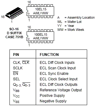
The EL15 features a multiplexed clock input to allow for the distribution of a lower speed scan or test clock along with the high speed system clock. When LOW (or left open and pulled LOW by the input pulldown resistor) the SEL pin will select the differential clock input.
The common enable (ENbar) is synchronous so that the outputs will only be enabled/disabled when they are already in the LOW state. This avoids any chance of generating a runt clock pulse when the device is enabled/disabled as can happen with an asynchronous control. The internal flip flop is clocked on the falling edge of the input clock, therefore all associated specification limits are referenced to the negative edge of the clock input.
The 100 series contains temperature compensation.
output should be connected to the CLK input and bypassed to ground via a 0.01 F capacitor. The V
output is designed to act as the switching reference for the input of the EL15 under single-ended input conditions, as a result this pin can only source/sink up to 0.5mA of current.
The EL15 features a multiplexed clock input to allow for the distribution of a lower speed scan or test clock along with the high speed system clock. When LOW (or left open and pulled LOW by the input pulldown resistor) the SEL pin will select the differential clock input.
The common enable (ENbar) is synchronous so that the outputs will only be enabled/disabled when they are already in the LOW state. This avoids any chance of generating a runt clock pulse when the device is enabled/disabled as can happen with an asynchronous control. The internal flip flop is clocked on the falling edge of the input clock, therefore all associated specification limits are referenced to the negative edge of the clock input.
The 100 series contains temperature compensation.
- 50ps Output-to-Output Skew
- Synchronous Enable/Disable
- Multiplexed Clock Input
- ESD Protection: > 1 KV HBM, > 100 V MM
- PECL Mode Operating Range: V
- = 4.2 V to 5.7 V with V
- = 0 V
- NECL Mode Operating Range: V
- = 0 V with V
- = -4.2 V to -5.7 V
- Internal Input Pulldown Resistors on CLKs, SCLK, SEL, and ENbar.
- Meets or Exceeds JEDEC Spec EIA/JESD78 IC Latchup Test
- Moisture Sensitivity Level 1
- For Additional Information, see Application Note AND8003/D
- Flammability Rating: UL-94 code V-0 @ 1/8", Oxygen Index 28 to 34
- Transistor Count = 103 devices
- Pb-Free Packages are Available
电路图、引脚图和封装图
MC100EL15电路图
技术资料
应用案例
深入剖析2.5 V/3.3 V ECL差分接收器/驱动器MC10LVEP16和MC100LV
2026-04-12
深度解析MC100LVEL16:3.3V ECL差分接收器的卓越性能与应用潜力
2026-03-13
EL156组成的胆机电路图
2007-11-19
2.5 V/3.3 V ECL差分接收器/驱动器MC10LVEP16与MC100LVEP16
2026-04-11
EL156自制电子管功放
2010-10-28
探秘3.3 V/5 V ECL差分接收器/驱动器MC10EP16与MC100EP16
2026-04-11
EL156电子管制作的功放电路
2009-11-19
深入解析MC100EL17:5V ECL 四通道差分接收器
2026-04-11