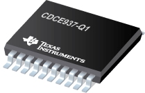
CDCE937-Q1
具有 2.5V 或 3.3V LVCMOS 输出的汽车类可编程 3-PLL VCXO 时钟合成器
制造商:TI
产品信息
描述 The CDCE937-Q1 and CDCEL937-Q1 devices are modular, phase-locked loop (PLL) based programmable clock synthesizers. These devices provide flexible and programmable options, such as output clocks, input signals, and control pins, so that the user can configure the CDCEx937-Q1 for their own specifications. The CDCEx937-Q1 generates up to seven output clocks from a single input frequency to enable both board space and cost savings. Additionally, with multiple outputs, the clock generator can replace multiple crystals with one clock generator. This makes the device well-suited for head unit and telematics applications in infotainment and camera systems in ADAS as these platforms are evolving into smaller and more cost effective systems. Furthermore, each output can be programmed in-system for any clock frequency up to 230 MHz through the integrated, configurable PLL. The PLL also supports spread-spectrum clocking (SSC) with programmable down and center spread. This provides better electromagnetic interference (EMI) performance to enable customers to pass industry standards such as CISPR-25. Customization of frequency programming and SSC are accessed using three user-defined control pins. This eliminates the additional interface requirement to control the clock. Specific power-up and power-down sequences can also be defined to the userΩs needs.特性Qualified for Automotive Applications AEC-Q100 Qualified With the Following Results: Device Temperature Grade 1: –40°C to 125°C Ambient Operating Temperature RangeDevice HBM ESD Classification Level 2 Device CDM ESD Classification Level C4B In-System Programmability and EEPROM Serial Programmable Volatile RegisterNonvolatile EEPROM to Store Customer Setting Flexible Input Clocking Concept External Crystal: 8 MHz to 32 MHzOn-Chip VCXO: Pull Range ±150 ppmSingle-Ended LVCMOS up to 160 MHz Free Selectable Output Frequency up to 230 MHz Low-Noise PLL Core Integrated PLL Loop Filter ComponentsLow Period Jitter (Typical 60 ps) Separate Output Supply Pins CDCE937-Q1: 3.3 V and 2.5 V CDCEL937-Q1: 1.8 V Flexible Clock Driver Three User-Definable Control Inputs [S0/S1/S2]; for Example: SSC Selection, Frequency Switching, Output Enable or Power DownGenerates Highly Accurate Clocks for Video, Audio, USB, IEEE1394, RFID, Bluetooth™, WLAN, Ethernet™, and GPSGenerates Common Clock Frequencies Used With TI-DaVinci™, OMAP™, DSPsProgrammable SSC ModulationEnables 0-PPM Clock Generation 1.8-V Device Power Supply Wide Temperature Range –40°C to 125°C Packaged in TSSOP Development and Programming Kit for Easy PLL Design and Programming (TI Pro-Clock™)APPLICATIONSClusters Head Units Navigation Systems Advanced Driver Assistance Systems (ADAS)All other trademarks are the property of their respective owners.
在线购买
型号:CDCE937QPWRQ1
描述:-
技术资料
应用案例
2024年Q1全球动力电池装机量152.2GWh
2024-05-24
汽车级多路复用器TMUX13xxA - Q1:特性、应用与设计要点
2026-01-13
从明月中提取灵感,鸿雁Q1胧悦系列开关优雅上市
2023-01-07
汽车级多路复用器TMUX13xxA - Q1:特性、应用与设计要点
2026-01-12
汽车应用新宠:TSDxx - Q1单向TVS二极管解析
2026-02-25
汽车应用的得力助手——TSDxx - Q1单向TVS二极管
2026-02-25
英威腾携两大利器亮相CDCE国际数据中心展会
2023-11-16
CDCE 2023国际数据中心展,华为数字能源邀您莅临参观
2023-11-11

