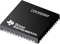
CDCE62005
具有集成双路 VCO 的 5/10 路输出时钟发生器/抖动消除器
制造商:TI
产品信息
描述 The CDCE62005 is a high performance clock generator and distributor featuring low output jitter, a high degree of configurability via a SPI interface, and programmable start up modes determined by on-chip EEPROM. Specifically tailored for clocking data converters and high-speed digital signals, the CDCE62005 achieves jitter performance well under 1 ps RMS (10 kHz to 20 MHz integration bandwidth).The CDCE62005 incorporates a synthesizer block with partially integrated loop filter, a clock distribution block including programmable output formats, and an input block featuring an innovative smart multiplexer. The clock distribution block includes five individually programmable outputs that can be configured to provide different combinations of output formats (LVPECL, LVDS, LVCMOS). Each output can also be programmed to a unique output frequency (up to 1.5 GHz) and skew relationship via a programmable delay block (note that frequency range depends on operational mode and output format selected). If all outputs are configured in single-ended mode (for example, LVCMOS), the CDCE62005 supports up to ten outputs. Each output can select one of four clock sources to condition and distribute including any of the three clock inputs or the output of the frequency synthesizer. The input block includes two universal differential inputs which support frequencies in the range of 40 kHz to 500 MHz and an auxiliary input that can be configured to connect to an external crystal via an on chip oscillator block.The smart input multiplexer has two modes of operation, manual and automatic. In manual mode, the user selects the synthesizer reference via the SPI interface. In automatic mode, the input multiplexer will automatically select between the highest priority input clock available.特性Superior Performance: Low Noise Clock Generator: 550 fs rms typical (10 kHz to 20 MHz Integration Bandwidth), FC = 100 MHz Low Noise Jitter Cleaner: 2.6 ps rms typical (10 kHz to 20 MHz Integration Bandwidth), FC = 100 MHz Flexible Frequency Planning: 5 Fully Configurable Outputs: LVPECL, LVDS, LVCMOS and Special High Swing Output Modes Unique Dual-VCO Architecture Supports a Wide Tuning Range: 1.750 GHz to 2.356 GHz Output Frequency Ranges from 4.25 MHz to 1.175 GHz in Synthesizer Mode Output Frequency up to 1.5 GHz in Fan-Out Mode Independent Coarse Skew Control on all Outputs High Flexibility: Integrated EEPROM Determines Device Configuration at Power-up Smart Input Multiplexer Automatically Switches Between One of Three Reference Inputs 7-mm × 7-mm 48-Pin VQFN Package (RGZ) 40°C to +85°C Temperature Range
应用案例
智能电网的核心是什么 智能电网的应用有哪些
2023-04-09
CDCE62005 时钟发生器芯片技术文档总结
2025-09-18
9月回顾丨一周快讯【145期】机智云入选广东智能制造生态合作伙伴/虎嗅大鲸榜工业AI TOP30
2023-11-25
第五代英特尔® 至强® 可扩展处理器助力星环科技分布式向量数据库 Transwarp Hippo 实现大幅性能提升
2023-12-17
ChatGPT是什么
2023-02-14
芯动力科技论文入选ISCA 2024,与国际巨头同台交流研究成果
2024-07-18
智芯半导体成功完成B轮融资
2024-10-23
接口兼容性陷阱:聚徽厂家解码RS232/RS485/CAN总线如何匹配设备联动
2025-07-12

