ADP5003
Low Noise μPMU 3 A Buck Regulator with 3 A LDO
制造商:ADI/AD
产品信息
优势和特点
Highly efficient low noise DC power supply system
High efficiency buck for first stage conversion
High PSRR, low noise LDO to remove switching ripple
Adaptive LDO headroom control option for optimal efficiency and PSRR across full load range
3 A Low-Noise Buck Regulator
Wide Input Voltage Range: 4.2 V to 15 V
Programmable Output Voltage Range: 0.6 V to 5 V
< 40 uVrms Output Noise (Independent of output voltage)
300 kHz to 2.5 MHz Internal clock with external sync up to
26 MHz (factory programmable divider)
3 A Low-Noise NFET LDO (Active Filter)
Wide Input Voltage Range: 0.65 V to 5 V
Fixed/Programmable Output Voltage Range: 0.6 V to 3.3 V
Differential Point of Load Remote-Sensing
< 10 uVrms Output Noise (independent of output voltage)
PSRR > 50 dB (to 100 kHz) with 300 mV headroom at 3 A
Ultra-Fast Transient Response
Power Good Output
Precision Enable Inputs for both the Buck Regulator and LDO
−40 °C to +125 °C junction temperature
32-lead 5 mm x 5 mm LFCSP Package
产品详情
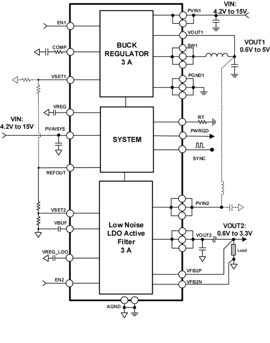
ADP5003 integrates a high voltage buck regulator and an ultralow noise low dropout (LDO) regulator in a small 5mm x 5mm LFCSP 32 lead package to provide highly efficient and quiet regulated supplies.
The buck regulator is optimized to operate at high output currents up to 3 A. The LDO is capable of a maximum output current of 3 A and is designed to operate efficiently with low headroom voltage while maintaining high power supplyrejection for frequencies as high as 1MHz.
ADP5003 can be configured to operate in one of two modes. The adaptive mode allows the LDO to operate with a set headroom by adjusting the buck output voltage internally. Alternatively ADP5003 can operate in an independent modewhere both regulators operate separately from each other and where the output voltages are programmed using resistor dividers.
The LDO output voltage can be accurately controlled at the point of load (POL) using the remote sense which compensates for PCB trace impedance while delivering high output currents.
Each regulator is activated via a dedicated precision enable input. The buck switching frequency can be synchronized to an external signal, or programmed with an external resistor.
Safety features in the ADP5003 include thermal shutdown (TSD) and input undervoltage lockout (UVLO). The ADP5003 is rated for a −40°C to +125°C junction temperature range.
Applications
Low noise power for High Speed ADC and DAC designs
Powering RF Agile Transceiver and Clocking ICs
电路图、引脚图和封装图
在线购买
型号:ADP5003ACPZ-R7
描述:-
应用案例
洞察电机驱动核心:利用PKDV5003进行变频器与伺服驱动器调试
2025-12-29
赋能绿色能源:PKDV5003在光伏逆变器与储能系统测试中的应用
2025-12-26
精准把脉开关电源:PKDV5003在电源拓扑关键节点测量中的应用
2025-12-24
霸菱科技智能门锁_ID-5003简介
2020-01-10
低压差线性稳压器ADP1712/ADP1713/ADP1714介绍
2023-07-07
拥抱高效能源转换:ERS5003ATT6升压DC/DC调节器引领绿色能源革命
2023-06-29
PFC控制器ADP1047/ADP1048的特性及典型应用电路
2021-03-11
DS5003安全微处理器芯片技术手册
2025-05-15

