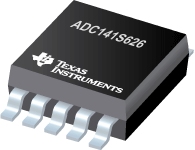
ADC141S626
14 位、50 kSPS 至 250 kSPS、差动输入、微功耗 A/D 转换器
制造商:TI
产品信息
描述 The ADC141S626 is a 14-bit, 50 kSPS to 250 kSPS sampling Analog-to-Digital (A/D) converter. The converter is based on a successive-approximation register (SAR) architecture where the differential nature of the analog inputs is maintained from the internal sample-and-hold circuits throughout the A/D converter to provide excellent common-mode signal rejection. The ADC141S626 features an external reference that can be varied from 1.0V to VA. It also features a zero-power track mode where the ADC is consuming the minimum amount of supply current while the internal sampling capacitor is tracking the applied analog input voltage.The serial data output is binary 2's complement and is compatible with several standards, such as SPI™, QSPI™, MICROWIRE, and many common DSP serial interfaces. The conversion result is clocked out by the serial clock input and is the result of the conversion currently in progress; thus, ADC141S626 has no latency.The ADC141S626 may be operated with independent analog (VA) and digital input/output (VIO) supplies. VA and VIO can range from 2.7V to 5.5V and can be set independent of each other. This allows a user to maximize performance and minimize power consumption by operating the analog portion of the ADC at a VA of 5V while communicating with a 3V controller on the digital side. With a 3V source, the power consumption when operating at 200 kSPS is 2.0 mW. With a 5V source, the power consumption when operating at 250 kSPS is 4.8 mW. The power consumption drops down to 4 µW and 13 µW respectively when the ADC141S626 enters acquisition (power-down) mode. The differential input, low power consumption, and small size make the ADC141S626 ideal for direct connection to bridge sensors and transducers in battery operated systems or remote data acquisition applications. Operation is guaranteed over the temperature range of −40°C to +85°C and clock rates of 0.9 MHz to 4.5 MHz. The ADC141S626 is available in a 10-lead VSSOP package.特性True Differential Inputs Guaranteed Performance from 50 kSPS to 250 kSPS External Reference Zero-Power Track Mode Wide Input Common-Mode Voltage Range Operating Temperature Range of −40°C to +85°C SPI™/QSPI™/MICROWIRE/DSP Compatible Serial Interface Key Specifications Conversion Rate: 50 kSPS to 250 kSPS INL: ± 0.95 LSB (Max) DNL: ± 0.95 LSB (Max) SNR: 82 dBc (Max) THD: -90 dBc (Typ) ENOB: 13.3 Bits(Min) Power Consumption:200 kSPS, 3V: 2.0 mW (Typ)250 kSPS, 5V: 4.8 mW (Typ)Power-Down, 3V: 4 µW (Typ)Power-Down, 5V: 13 µW (Typ) All trademarks are the property of their respective owners.
应用案例
ADC128S052:高性能12位A/D转换器的深度解析
2025-11-30
深入解析 ADC141S626:高性能低功耗的 A/D 转换器
2025-11-27
探索 ADC122S706:高性能双路 12 位 ADC 的卓越之旅
2025-11-27
adc0832是什么_adc0832和adc0809区别
2020-04-26
adc0832时序图_adc0832怎么转换光敏电阻
2020-04-26
OPA141 单通道、10MHz、单电源、低噪声、JFET精密放大器技术手册
2025-05-12
A626**高效3A同步整流降压转换器输出电流SOT23-6封装
2024-05-17
高通653/626手机处理器订单 台积电/三星瓜分
2016-10-24

